Increases in component packaging density and the demand for more functionality have continued to drive design rules toward achieving a higher and higher interconnection density. You will find some valuable results and capabilites of a performed customer evaluation project for the advanced depth routing use of a routing system.
The market’s demands for finer structures have grown considerably over the years. Aside from smaller components, PCB dimensions for rigid and flex circuits have become increasingly smaller and lighter. Therefore, the products have been made smaller and faster. In effect, one technology has been a driver for the other. As miniaturization trends continue this course will make technological improvement and design creativity in the PCB production process indispensable.
In the context of drilling and routing, laser technology has enjoyed a fair share of publicity. For a long time, some considered laser technology to be the replacement for traditional mechanical processing. Lasers might play a leading role in current and future market demands, but there still are a lot of questions to be answered and a long way to go in terms of productivity and flexible capabilities.
The new market specifications for precision and tolerance can be supported by mechanical processes. Mechanical circuit board processes however have some advantages like easy adjustments or lower costs. Over the years mechanical drilling and routing had been developed quite significantly. There is a new generation of demand in the market for system capabilities, tolerances and applications. The market shows a trend to flex and flex-rigid boards. Certain microwave designs where relatively large surface areas have to be crossed is a special challenge for routing and controlled-depth milling. All of this displays a clear trend towards multiplicity and flexibility which needs to be offered by equipment manufacturers.
The Swiss machine analyzed below, allows depth routing with an accuracy of +/- 15.0 um. Up to now, this seemed impossible with the focus being only on laser technology. However the strength of a drilling machine is still accuracy based performance. The depth routing option allows for very complex designs, bended boards and structures to be processed with fine precision.
Depth routing technology- applications
Option 1 is routing the top of the surface
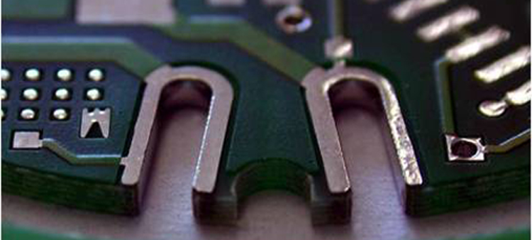
Pocket routing for components is used on rigid-flexible Printed Circuit Boards. The top surface will be milled away (taking the height of the chip and board into account). Considering a larger area must be traversed, the detection of the real surface structure is a key element. With non conductive top surfaces a 2nd measuring system is needed. Different detection and calculation methods, (see below), can be used. An accuracy of +-40 um is achievable with non conductive surfaces and +- 15 um on conductive spots. Pocket routing is mainly used if you need smaller boards and a lower board thickness for buried processors or resistors.
Option 2 is routing down to the innerlayers
In some applications a board needs to be designed with grounded innerlayers and free contact surfaces on an innerlayer, which are required to be connected to a chip. Designs should avoid tracks around the hole and above the chip. A nearby contact could falsely report the system as a closed loop and cause a false measurement, guiding the spindle to an undesired position. Customers currently use up to 12 layers in standard practice and production. The main reason for OEMs to use this kind of design is space, speed (shorter tracks) and EMC requirements. Technology-wise there are no limitations in layer count. As more layers are added, it becomes more difficult for the system to detect the right target layer and to measure the depth.
This type of depth routing technology allows designers to sink in a chip below the board surface and design a second chip above it. Routing leaves a square donut in between the connections of the two chips. Accuracy is within +/-15 um.
This advanced design causes less EMC problems due to the symmetry and the short distance between the components instead of using long tracks to connect them. But the real challenge is to evacuate the heat from in between the two components. This issue can be addressed by implementing an air channel and the integration of heat pipes.
Option 3 is routing semi flexible FR4 and rigid-flexible PCBs
Depth routing for semi flexible FR4 and rigid-flexible boards will be used if your board designer requests a bended board (which can be folded once). A part of the board will be milled away with an accuracy of +-20 um. As a result, the board can be bended, less space is needed and the product therefore can be smaller in size. Because there is no conductive area in which to measure, the table of the drilling/ routing machine will be used to detect the depth (detection methods see below).
In Conclusion
Mechanical routing technology is ideal for PCB manufacturers who target high tech markets and prepare themselves for the customer’s demands of today and tomorrow. Depth routing technology supports a high end market with the need for accuracy, miniaturization, process stability and the need for productivity.
Key markets for routing technology include: telecommunications, automotive as well as niche markets such as aerospace.
A significant advantage of the mechanical routing process is flexibility. Mechanical routing processes can offer a wide range of applications and the use of organic and non-organic materials like polyimide or exposy resins, copper – brass PCB with ceramic insulation layer and alloy (aerospace products). Routing with oil mist for non-ferrous materials is also available.
Automatic tool changes and spindle direction turns (reversed rotation) offer accuracy and productivity. Due to this fact, burr issues will be reduced by routing from both sides. The different applications and detection methods to control depth offer a wide range of products which can be utilised.
The Swiss Equipment manufacturer developed a sophisticated interpolation algorithm which improves the accuracy and productivity while routing complex contours. This method also considerably reduces the tool wear and increases the lifetime of the routing tool.
To use the described design options, some depth routing manufacturing know-how and the right equipment is necessary. Therefore a close relationship between designers and PCB manufacturers has proven to be helpful.
Moreover, in various markets there is a rising demand for this kind of high-end technology. And as of today, some PCB shops and markets might stand a better chance to differentiate themselves from their competitors.